Clone PCB circuit board is PCB copy board, PCB copy board is PCB circuit board clone, is the reverse engineering of PCB circuit board design. Firstly, the components on the PCB circuit board are removed to make BOM single, and the empty PCB board is scanned into a picture, which is processed by the board software and restored to the pcb board file. Send pcb board drawing file to PCB board factory to make board (PCBA). Purchase the corresponding components according to the BOM. Re-solder the electronic components. This is the same as the original PCB circuit board PCB circuit board.
Through the PCB copy board technology can complete any electronic product imitation, electronic product clone.
Copy PCB board is also called to change the board, is the design of the PCB board for reverse technology research. In reference to a lot of information.If you need PCB copy service please contact China Shenzhen OROD Technology.
What is the process of PCB copy board service?
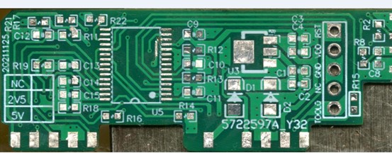
Step 1: Get a functioning and intact PCB board , first record the model, parameters, and location of all components on the paper. Especially the direction of the diode, the triplet, the direction of the IC notch. It is best to use an HD camera to take two pictures of the position of the element. Now pcb circuit board more and more advanced. If you don’t pay attention to the diodes on the top, the triode is a little hard to see.
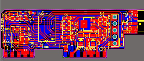
Step 2: Remove all components and parts and the tin in the PAD hole. The PCB was cleaned with alcohol and then placed inside the scanner. The scanner needs to turn up the pixels slightly to get a sharper image. Then the top and bottom layers are slightly polished with water yarn paper until the copper film is bright, put into the scanner, Open PCB copy assistant software “PHOTOSHOP” , and sweep the two layers into the color way. Note that the PCB must be placed horizontally and vertically in the scanner, otherwise the scanned image cannot be used.
Step 3: Adjust the contrast, light and shade of the canvas, so that the part with copper film and the part without copper film contrast strongly. Then turn the secondary figure to black and white to check whether the lines are clear, if not, repeat this step. If it is clear, save the image as a black and white BMP format file TOP.BMP and BOT.BMP. If there is a problem with the graphics can also use “PHOTOSHOP” to repair and correct.
Step 4: Convert the two BMP format files to PCB copy software “PROTEL” format files. Loading two layers in “PROTEL”, such as PAD and VIA after two layers basically coincide, indicating that the first few steps are done well, if there is deviation, repeat the third step. Therefore, pcb copy board is a very patient work, because a small problem will affect the quality and the matching degree after the PCB copy board.
Step 5: Convert the BMP of the TOP layer to Top.PCB, pay attention to the SILK layer, which is the yellow layer, and then you trace the line on the TOP layer, and place the device according to the drawing of the second step. Delete the SILK layer after painting. Repeat until all layers have been painted.