
Look, the semiconductor has an essential role in manufacturing. When we dive into its component, it displays the central importance of multiple trends in the automotive industry. The chemical element gets processed in the wafer form in the semiconductor production. Those wafers are built up within the plastic cassettes during the production time under certain circumstances and can be made further step by step. Due to the multifold in the semiconductor request, manufacturers wish to automate the process from the other end. You know the rising manufacturing process while looking upon the cleanliness and the environmental control is considered the wafer handling equipment. It has risen out from the semiconductor devices manufacturing within the semiconductor front end manufacturing industry. This process is made out for the specific environments where the temperature, humidity, and particle contamination have been checked upon and regulated within particular parameters.
How can Wafer Handling Automation benefit the Semiconductor Manufacturing Industry?
- Properly distribution of the chemicals
- No requirement of the meters
- High in the quality prospects
- Very budget-friendly option
How do the customers get to drive towards Wafer Handling?
- Low energy consumption
- 360 degrees rotation
- Ergonomic design
- Easy to load and fill
- Personalized controls
The Kensington Laboratories cater to the customized form of motion controls, robotics, load port, as well as the precision level in a rigorous manner. The newest functionalities of the wafer handling equipment, as well as stage repairs, present a single solution to build up the semiconductors’ performances.
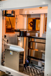
The wafer handling robots can light upon the needs of the semiconductors quartz and wafer handling for so long. The semiconductor robot handling and the wafer handling depicts an important feature of the beam wafer sensing with the wafer handling robots. Moreover, the wafer handling robots are made in use in the semiconductor equipment spectrum for several processes like thermal processing systems, deposition systems, metrology, and many other systems in a case.
Let us talk about the features of the wafer handling robot WFH series:
- Proven reliability in the two decades of the semiconductor equipment wafer handler applications.
- Real-time force sensing over entire axes for the operator and the water safety
- The cleanliness surpassing Class 1, semiconductor equipment needs
- The wafer handler robot with unmatched throughput, reliability as well as precision.
- Easy in using high-level commands, self-teaching, and extensive fault and recovery intelligence.
- The integral or off-axis pre-aligner or barcode reader.
- The direct optical encoding of the entire axes yields wafer placement repeatability.
- Availability of the 3 to 8 semiconductor wafer capability with not at all electromechanical changeovers.
- It can be well-integrated with the Kensingtons’ extraordinary architecture of precision motion control equipment.
- It is capable of building integrated and supportable automated wafer handling robot systems economically.
In fact, wafer handling end effectors have a long history of semiconductor wafer fabrication operations. The Kensington end effectors innovations have advanced wafer processing capability. These further include 300mm edge grip for narrowing the particle performance as well as through-beam technology for the wafer mapping process.
The Kensington Laboratories holds a focus on the cutting edge semiconductor technology that helps in the future applications to widen further. This can actually fulfill the entire requirements while generating changes in the semiconductor assembly and the semiconductor front end manufacturing strategies. We proudly build and deliver a broad range of wafer handling solutions from the normal equipment front end modules (EFEM) to the automation platforms. Whatever wafer handling application or custom solution you are looking for, we will engineer all kinds of solutions to fulfill your wafer handling requirements. Suppose you let us integrate the latest advancements in the wafer handling technologies. In that case, we will help you get high-performance wafer and substrate handling solutions, which help to streamline the semiconductor manufacturing process.
Get to partner with us today and look up to for the improvised yield, throughput as well as exceptional customer service.