
Manufacturing Printed Circuit Boards (PCBs) has always been a tremendously complicated and expensive process. The “real” cost of manufacturing PCBs increases when you add faulty components to the mix. The pandemic triggered a higher-than-expected demand for new PCBs. These demands lead to shortages of essential PCB raw materials like copper foils, aluminum (for metal-backed PCBs), etc.
For PCB manufacturers and their supply bases, things couldn’t be more challenging. Their lead times are being stretched. The cost of manufacturing PCBs is constantly increasing. How long will it take for the prices of PCB components to return to normal levels? In early 2021, experts claimed that these shortages would ease by 2022. Now, those forecasts seem to be over-optimistic. Global PCB material supply shortages will prevail for many more years.
Many PCB companies are reducing their production expectations. Other companies are following precise PCB design and manufacturing processes. Unfortunately, no matter how efficient PCB manufacturers are, the risk of defects, bugs, and other human errors is ever-present. Identifying and addressing these risks during early production stages is critical for ensuring the consistency and reliability of PCBs.
That means having a strict approach to PCB testing and inspection. Proper testing and inspection are the only ways PCB manufacturers can ensure the supply of top-quality, long-lasting products. Discussed below are the best PCB inspection methods that should be undertaken by all PCB professionals. Carrying out these inspection techniques will streamline their production cycles in the post-pandemic world.
The Latest PCB Testing and Inspection Techniques
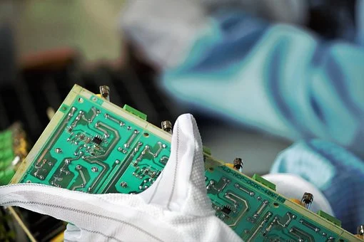
PCB testing and inspection processes vary based on the types of PCBs being tested. These are the factors PCB inspection experts consider before prescribing specific tests and inspections –
- The type of PCB being tested (single-sided PCBs, multilayer PCBs, rigid PCBs, flex PCBs, etc.)
- The application of the PCB (which electronic device will the PCB be used on)
- The sensitivity and tolerance ratings of the PCBs.
For instance, PCBs designed for medical or military devices require stricter reliability testing than PCBs designed for household electronic appliances. Top PCB inspection experts combine various testing techniques to provide the most accurate analysis of potential defects in the boards.
All PCB inspection experts follow the IPC-A-610 standard while inspecting and testing PCBs. This document called “Acceptability of Electronic Assemblies” provides workers with testing and inspection guidelines that are followed across the globe.
Professionals who receive IPC-A-610 training know what quality standards they need to maintain. From hands-on inspections to using the latest testing tools – workers learn it all when they get their IPC-A-610 certifications.
Here are some of the latest PCB testing and inspection techniques that the best IPC-A-610-certified professionals employ:
- In-Circuit Testing: In-Circuit Testing (ICT) is the process of checking the integrity of the soldered connections on the boards. These tests detect most defects that occur during PCB manufacturing processes (up to 98% of manufacturing faults). Inspection experts ensure that each component produced matches the original PCB designs. This easy-to-interpret testing technique is ideal for large batches of PCBs where manufacturers expect very few amendments and repairs.
- Flying Probe Tests: Flying probe tests check for diode issues, inductance or capacitance issues, shorts, and opens on PCBs. PCB inspection experts use elements with smaller pitches (less than 0.2mm) to test PCB components and SMD pins. Flying probe testing is cheaper than ICT.
- Automated Optical Inspection: Very few companies have access to AOI tools. AOI inspection involves the use of 3D cameras to optically analyze the designs of the PCBs being manufactured. The AOI tool’s advanced software compares the images from the PCBs under the test cameras with the original designs. If any board doesn’t precisely match the original design, it’s marked for human inspection. AOI is time-efficient and perhaps the best inspection technique for detecting early-stage issues inside PCBs. Most companies that own AOI tools use them in conjunction with other tests and inspections. For instance, a PCB manufacturer may conduct AOI and ICT.
- X-Ray Inspection: This relatively old inspection technique enables PCB technicians to locate potential defects early on in the manufacturing process. The X-ray devices allow them to look closely at soldered connections, internal traces, and other small details. This technique is ideal for reviewing the boards and their multiple layers. Inspection experts also get to double-verify the quality of soldering on the PCBs and the alignment of other board components.
Choosing the Right PCB Testing Solutions
PCB inspection experts who know the testing requirements mentioned in the IPC-A-610 document will find these processes easy. That’s because IPC-A-610 certification makes workers more familiar with the materials and subcomponents used to make PCBs. Workers who receive IPC-A-610 training also learn –
- Visual PCB inspection strategies
- Functional Testing (FCT)
- Through-hole inspection
- Wire and terminal inspection
- SMT and BGA inspection
In the post-pandemic world, identifying and resolving PCB faults like short circuits, poor soldering, etc., will be the priority of manufacturers. That’s why keeping up with the latest PCB testing, and inspection techniques is vital for them.