

Since its inception, silicon chip technology has consistently developed in accordance with Moore’s Law. As the size of the device continues to shrink, the transistor channel is also constantly shortened. But when the channel is shortened to a certain extent, quantum tunneling is very easy to occur. As a result, even if no voltage is applied, electrons can freely travel between the source and the drain, making the transistor lose its switching function. In order to break through the 22nm process limit, FinFET came into being.
The working principle of FinFET
In the traditional transistor structure, the gate that controls the flow of current can only control the on and off of the circuit on one side of the gate, which is a planar structure. In the FinFET architecture, the gate is a fork-shaped 3D architecture similar to a fish fin, and the on and off of the circuit can be controlled on both sides of the circuit.
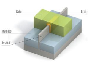
The figure shows the structure diagram of the FinFET. The gate surrounds the channel from three sides, and the three-dimensional structure replaces the planar device to enhance the control ability of the gate. After the voltage is applied, an inversion layer conduction channel is formed under the gate oxide layer like a traditional transistor to control the flow of carriers, so as to achieve its most basic switching function.
The working principle of FinFET
The difference between FinFET and traditional planar devices
1. The channel of FinFET is generally lightly doped or even undoped. It avoids the scattering effect of discrete doped atoms. Compared with heavily doped planar devices, its carrier mobility will be much greater. improve.
2. The FinFET mechanism increases the control area of the gate to the channel, which greatly enhances the gate control ability, which can effectively suppress the short channel effect and reduce the subthreshold leakage current. The sub-threshold swing S is a performance index that measures the conversion rate between the turn-on and turn-off states of a transistor. It represents the change in the gate voltage required for a ten-fold change in the source-drain current. The smaller S means the faster the turn-on and turn-off rate. At present, the limit value of S at room temperature is about 60mV/dec, and it is difficult to reduce as the size of the device shrinks. In FinFET, as the thickness of silicon Fin decreases, the sub-threshold slope also decreases and approaches the ideal value of 60mV/dec. This is because as the thickness of the silicon Fin decreases, the gate’s ability to control the channel will gradually increase, and the suppression of the short channel effect will also become greater.
3. Due to the suppression of the short channel effect and the enhancement of the gate control capability, the FinFET device can use a thicker gate oxide than the planar device, thereby reducing the gate leakage current.
4. A stronger gate control capability allows the gate length of the transistor to be greatly shortened, thereby further reducing the area.
On the whole, compared with planar devices, FINFET structure has better channel control capability and better sub-threshold slope, which can provide smaller leakage current and smaller gate delay as well as greater current drive capability. It has many advantages and has a good application prospect in the 22nm technology generation and below.
Manufacturing process
There are currently two substrate solutions to choose from:
Bulk silicon substrate: There may be a source-drain punch-through problem. The process is more cumbersome and requires steps such as etching bulk silicon-depositing an insulating layer-CMP. And need to provide additional isolation.
Solution: Use a heavy doping process under the trench to form a punch-through barrier layer; form a local buried oxygen isolation under the source and drain.
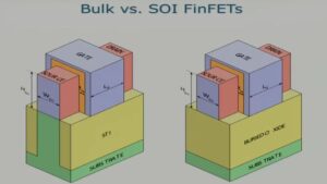
SOI substrate: Due to the buried oxide layer, it is easier to fabricate FinFET on SOI substrate, and natural electrical isolation is formed between source and drain and between devices, which can effectively suppress leakage and avoid latch-up effects. The delay and dynamic power consumption of the device are lower. However, SOI substrates have problems such as high wafer cost, high defect density, and poor heat dissipation. The thermal conductivity of silicon dioxide is low. The existence of the buried oxide layer of the SOI substrate prevents the heat generated by the device from rapidly diffusing out and accumulating in the channel, which increases the temperature of the device, and the mobility, threshold voltage, drain current of the device, The sub-threshold swing will be affected by temperature.
Solution: Use new insulating and low thermal resistance materials. Using molecular beam epitaxy MBE technology, thereby reducing the defect density of the epitaxial insulating layer.
Here you can refer to another article about FinFET.