
A Printed Circuit Board (PCB) resembles the form of a sandwich and consists of both conducting and insulating layers that are bonded together. Adding solder paste to the board, picking and placing components, soldering, inspection, and testing are all phases in the PCB manufacturing process. All of these steps are essential and must be monitored to guarantee that the best quality product is generated. A full turn key PCB assembly procedure detailed below presupposes the use of surface mount components, as surface mount technology is now employed in almost all PCB manufacturing.
A fully assembled PCB is one that has all components fully installed, and the manufacturing process is known as Quick turn PCB assembly, which is abbreviated to PCBA. Traces are the names for the copper wires on a bare board that forms electrical connections between components and connect with signals, which give instructions to the circuit board. PCBs can range in sophistication, from very simple to extremely complex, and they can be as small as a human thumbnail in size.
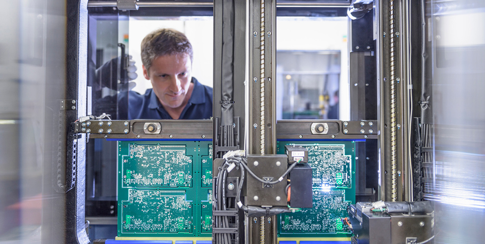
Quick turn PCB assembly is the process of transforming a bare PCB board, into one that has all of its electrical components and traces in place. PCBA production and testing are also offered by PCB manufacturers.
The PCBA process always begins with the most basic element of the PCB: the base, which is made up of multiple layers, each of which plays an important part in a final PCB’s functioning. The following layers alternate:
- Substrate: A PCB’s foundation material. It is responsible for the stiffness of the PCB.
- Copper: A thin coating of conductive copper foil is applied to each functional side of the PCB — one side of the PCB is single-sided, or both sides of the PCB is double-sided. This forms the copper traces layers.
For more information, visit us.